Datasheet4U.com - HYMP125U64CP8-S5

HYMP125U64CP8-S5 Datasheet, Hynix Semiconductor

HYMP125U64CP8-S5 Datasheet, Hynix Semiconductor

Page 1 of HYMP125U64CP8-S5 Page 2 of HYMP125U64CP8-S5 Page 3 of HYMP125U64CP8-S5

HYMP125U64CP8-S5 version equivalent

  • 240pin ddr2 sdram unbuffered dimms based on 1gb c version.
  • Preview is limited to up to three pages.

HYMP125U64CP8-S5 Features and benefits

HYMP125U64CP8-S5 Features and benefits


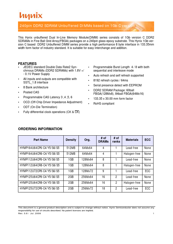
* JEDEC standard Double Data Rate2 Synchrnous DRAMs (DDR2 SDRAMs) with 1.8V +/ - 0.1V Power Supply All inputs and outputs are compatible with SSTL_1.8 interface 8 Ban.

HYMP125U64CP8-S5 Description

HYMP125U64CP8-S5 Description

and is subject to change without notice. Hynix Semiconductor does not assume any responsibility for use of circuits described. No patent licenses are implied. Rev. 0.6 / Jul. 2008 1 
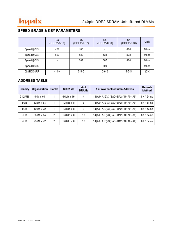
1240pin DDR2 SDRAM Unbuffered DIMMs SPEED GRADE & KEY PARAMETERS C4.

Image gallery

Page 1 of HYMP125U64CP8-S5 Page 2 of HYMP125U64CP8-S5 Page 3 of HYMP125U64CP8-S5

TAGS

HYMP125U64CP8-S5
240pin
DDR2
SDRAM
Unbuffered
DIMMs
based
1Gb
version
Hynix Semiconductor

Manufacturer


Hynix Semiconductor

Related datasheet

HYMP125U64CP8-S6

HYMP125U64CP8-C4

HYMP125U64CP8-Y5

HYMP125U64CR8-C4

HYMP125U64CR8-S5

HYMP125U64CR8-S6

HYMP125U64CR8-Y5

HYMP125U72CP8-C4

HYMP125U72CP8-S5

HYMP125U72CP8-S6

Since 2006. D4U Semicon.   |   Datasheet4U.com   |   Contact Us   |   Privacy Policy   |   Purchase of parts